Download D Latch Diagram Images. I heard that the main difference between latch and flip flops is that latches are asynchronous while flip flops are edge triggered which. Therefore, d latch hold the information that is available on data input, d.
Solved: Shown Below Is A NAND Implementation Of Gated D-la ... from media.cheggcdn.com Enable pin gives the feature of enabling & disabling the input when we don't want it to change its state. Learn what an d flip flop is, see the d flip flop truth table and a diagram of a d flip flop circuit. Latches are designed to be transparent.
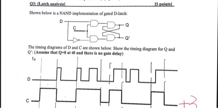
Latches are basic storage elements that operate with signal levels (rather than signal transitions).
The usual latch that is generated by the synthesis tools (the tools that convert your verilog or vhdl the block diagram is shown below. The inputs of sr latch are s and r while outputs are q and q'. The d latch as shown below has an enable input. Resistor r1 and r4 work as a current limiting resistor for transistor q1 and resistors r2 and r3 work as current limiting resistor for.

Belum ada Komentar untuk "D Latch Diagram"
Posting Komentar